Search...

Global semiconductor leader NXP Semiconductor recently revealed plans to cease all production activities at its longstanding factory in Nijmegen, Netherlands, along with the closure of three U.S.-based manufacturing sites.
This strategic move is part of NXP’s broader initiative to upgrade capacity and adopt more efficient production technologies at its newer facilities in Singapore and Germany, with completion expected over the next few years.
A Legacy Factory Comes to an End
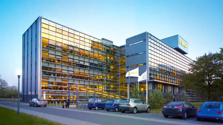
The Nijmegen factory has been a cornerstone of the Dutch semiconductor industry for decades.
Originally established during the Philips era, it remains NXP’s largest production site worldwide, employing approximately 1,700 people.
This factory has primarily focused on manufacturing chips for the automotive sector. However, the plant’s aging production technology—using 200mm (8-inch) wafers—lags behind modern standards, limiting output and efficiency.
Why the Shift to 300mm (12-inch) Wafers Matters
New factories employ the industry-standard 300mm (12-inch) wafers, which can produce significantly more chips per wafer.
In fact, a single 12-inch wafer offers about 2.25 times the surface area of an 8-inch wafer, allowing a far greater number of chips to be manufactured under the same conditions.
This translates into lower manufacturing costs and higher profit margins, key factors driving NXP’s transition.
Strategic Investments in Germany and Singapore
NXP’s new factory in Dresden, Germany, is a joint venture involving major industry players such as Infineon, Bosch, and TSMC, with NXP holding a 10% stake.
Meanwhile, the Singapore facility, currently under construction in partnership with Vanguard International Semiconductor Corporation (VIS), represents an even larger investment of approximately $7.8 billion USD, where NXP owns 40%.
This plant will focus on producing mixed-signal, power management, and analog chips ranging from 130nm to 40nm process nodes. Both factories are slated to begin full-scale operations by 2027.
Expanding Partnerships: Potential Manufacturing in India
Recent reports indicate that India’s Tata Electronics is negotiating with NXP to become a foundry partner, potentially manufacturing select NXP products at Tata’s 12-inch wafer facility in Gujarat.
This would mark another step in NXP’s global capacity expansion and supply chain diversification.
Industry-Wide Trends Reflected in NXP’s Strategy
NXP’s operational pivot is emblematic of a global semiconductor industry shift toward advanced manufacturing technologies driven by booming demand in AI, data centers, and IoT.
Larger wafer sizes not only improve material utilization but also dramatically reduce per-unit production costs. According to SEMI, between 2023 and 2026, 82 new 12-inch wafer fabs and production lines are planned worldwide, pushing global 12-inch wafer production capacity to an estimated 9.6 million wafers per month by 2026.
Conclusion
NXP’s move to phase out its legacy facilities in favor of modern, large-wafer factories underlines the relentless push for efficiency and innovation in semiconductor manufacturing.
For industry partners, customers, and investors, this signals NXP’s commitment to staying at the forefront of technology while optimizing cost structures and capacity for future growth.
 More information?
AXTEK Series NYQUEST CMSEMICON ST MICROELECTRONICS Featured Manufacturers Puya MCUs ICMAN Touch Chips ZXInfoTek Holtek MCUs MORNSUN Modules
Company Profile Certificates Terms & Conditions Privacy Statement


 MCU Solutions
 PCBA Solutions
 Bluetooth Solutions
 FAQ
FAQ Contact Us
 Company News
 Technology News
 Industry News
 PCBA News
 Company Profile
 Certificates
 Terms & Conditions
 Privacy Statement
 Home Appliances
 Beauty Appliances
 Lighting
 Kid's Toys
 Security Alarm
 Health Care