Search...

Voltage-to-current (V/I) conversion circuits are widely used in industrial environments, especially in 4–20 mA current loop systems. In this article, we will walk through the working principle and practical design of a high-side V/I converter circuit with a real-world example.
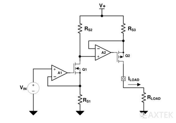
This high-side V/I conversion circuit provides a controllable current to a grounded load. It consists of a two-stage architecture:
Stage 1: Converts the input voltage (VIN) into a current reference using an op-amp and NMOS.
Stage 2: Uses a second op-amp to control the gate of a PMOS, thereby regulating the output current to the load.
The V-I transfer function is determined by the relationship between the input voltage VIN and three current-sensing resistors RS1, RS2, and RS3:
Stage 1:
VRS1=VIN→IRS1=RS1VIN
Stage 2:
IRS2≈IRS1,VRS3≈VRS2,ILOAD≈IRS3
Overall transfer function:
ILOAD=RS1VIN×RS2RS3
Supply Voltage: 5V DC
Input Voltage Range: 0–2V DC
Output: 4.5V / 0–100 mA current
Efficiency: ≥ 98%
Gain Error: ≤ 0.1%
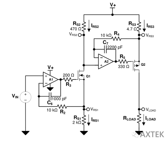
The first stage doesn't drive the load directly, so its power consumption affects overall efficiency. To limit losses and leave headroom for the op-amp's quiescent current, we set the first stage current (IRS1) to 1 mA when the output is at full-scale 100 mA.
Max VIN = 2V, so:
RS1=1mA2V=2kΩ
The second stage generates the output current to the load. Assuming the PMOS drop (VDS) is ~0.3V and aiming for 4.5V across the load (given 5V supply), the voltage across RS3 should be ~470 mV.
For IRS2 ≈ 1 mA:
RS2=1mA470mV=470Ω
For ILOAD = 100 mA:
RS3=100mA470mV=4.7Ω
Both op-amp stages require compensation to maintain stability. Driving capacitive loads like MOSFET gates can cause oscillation. This design uses a dual-feedback loop, a classic topology that stabilizes the output. For detailed implementation, refer to the technical notes on dual feedback compensation.
| Component | Selection Criteria | Notes |
| Op-Amp | Low offset, low drift, rail-to-rail I/O | e.g., TI OPA192, OPA2333; ADI ADA4522 |
| MOSFET | Low threshold (VGS(th)), high current rating | e.g., IRLML6402, IRLML6344 |
| Current-Sense Resistors | 0.1% tolerance, low temperature coefficient | Essential for gain accuracy ≤ 0.1% |
⚠️ Note: RS1 accuracy is especially critical, since its error is multiplied by the gain ratio RS3/RS2 and directly affects output current.
This two-stage high-side V/I converter design offers a precise and efficient method to translate a low-voltage analog input into a regulated current output for grounded loads. It is well-suited for applications such as:
Industrial sensor excitation
Analog signal transmission over long distances
Programmable current sources
With careful selection of op-amps, MOSFETs, and precision resistors, the circuit achieves:
√ High efficiency (≥98%)
√ Low gain error (≤0.1%)
√ Stable operation under capacitive load
 More information?
AXTEK Series NYQUEST CMSEMICON ST MICROELECTRONICS Featured Manufacturers Puya MCUs ICMAN Touch Chips ZXInfoTek Holtek MCUs MORNSUN Modules
Company Profile Certificates Terms & Conditions Privacy Statement


 MCU Solutions
 PCBA Solutions
 Bluetooth Solutions
 FAQ
FAQ Contact Us
 Company News
 Technology News
 Industry News
 PCBA News
 Company Profile
 Certificates
 Terms & Conditions
 Privacy Statement
 Home Appliances
 Beauty Appliances
 Lighting
 Kid's Toys
 Security Alarm
 Health Care