Search...

Supply voltage range: 2.0V to 5.5V
Temperature range: -40℃ to 125℃
Low power mode: sleep mode, deep sleep mode
Operating power consumption: 100uA/ MHz@64MHz
Power consumption in deep sleep mode: 1.5uA
Deep sleep mode +32.768K+RTC operation: 1.9uA
ARM®32-bit Cortex-M0®+ CPU
Operating frequency: 32KHz to 64MHz
512KB Flash memory, program sharedwith data storage
20KB dedicated data Flash memory
64KB SRAM MEMORY WITH PARITY
Built-in power-on reset (POL) circuitry
Built-in voltage detection (LVD) circuit(threshold voltage can be set).
Built-in high-speed oscillator, accuracy(±1%). 1MHz to 64MHz system clock andperipheral module action clock areavailable
Built-in 15KHz low-speed oscillator
Built-in 1 channel PLL
Support 1MHz ~ 20MHz external crystaloscillator, support stop vibrationmonitoring
Supports 32.768KHz external crystaloscillator for correction of internal high- speed oscillators
Multiplier: Supports single-cycle 32bitmultiplication operations
Divider: Supports 32bit signed integerdivision and requires only 8 CPU clockcycles to complete the operation
An interrupt triggers a start.
Transmission modes are selectable(normal transfer mode, repeat transfer mode, block transfer mode, and chaintransfer mode).
The source/destination field is optional forfull address space range
It can link event signals together toachieve the linkage of peripheralfunctions.
There are 23 types of event inputs and 10types of event triggers.
12-bit precision ADC converter with slewrate 1 42Msps, 28 external analogchannels, internal optional PGA output asa conversion channel, with temperaturesensor, support for single-channelconversion mode and 2, 3, 4-channelscanning conversion mode. Conversionrange: 0 to positive reference voltage
8-bit precision D/A converter, 2-channelanalog output, real-time output function, output voltage range 0~VDD
Comparator (CMP) with built-in two- channel hysteresis comparator, selectable input source, and selectableexternal or internal reference voltagereference
Programmable gain amplifier (PGA) withtwo channels of PGA to program4/8/10/12/14/16/32 gains with an externalGND pin that can be used as differentialmode
I/O ports: 59-93
Capable of N-channel open-drain, TTLinput buffering, and internal pull-upswitching
Built-in key interrupt check-out function
Control circuitry with built-in clockoutput/buzzer output
16-bit timer: 17 channels (with PWMfunction and motor dedicated PWMfunction).
15-bit interval timer: 1
Real-time clock (RTC): 1 (with perpetualcalendar, alarm clock function, andsupport for a wide range of clockcorrection).
Watchdog timer (WWDT): 1
SysTick timer
Three serial communication units: serialcommunication unit 0 can be freely configured as 2-channel standard UARTor 4-channel 3-wire SPI or 4-channelsimple I2C; Serial communication unit 1 or 2 can be freely configured as 1-channel standard UART or 2-channel 3-wire SPIor 2-channel simple I2C; (UART of unit 0supports LIN Bus communication, SPI00channel supports 4-wire SPIcommunication)
Standard SPI: 2 channels (supports 8-bitand 16-bit)
Standard I2C: 2 channels
CAN: 3 channels
LCD BUS interface: support 8080, 6800connectors
Complies with IEC/UL 60730 relatedstandards
Abnormal storage space access error is reported
Supports RAM parity
Supports hardware CRC verification
Supports critical SFR protection againstmisoperation
128-bit unique ID number
Flashsecondary protection in debug mode(Level1: only flash full-domain erasure, noread or write; Level2: The emulatorconnection is invalid and cannot beoperated on flash).
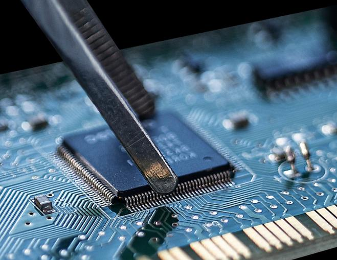
Support 64Pin, 80Pin, 100Pin multiplepackages
You can get your Automotive MCU BAT32A279 solution by flling out the form below and we will contact you immediately.
Puya MCUs ICMAN Touch Chips Holtek MCUs JL Bluetooth Chips Customized PCBA Design MORNSUN Cmsemicron MCUs Electornic Components Modules ZXInfoTek
Company Profile Certificates Terms & Conditions Privacy Statement


 MCU Solutions
 PCBA Solutions
 Bluetooth Solutions
 FAQ
FAQ Contact Us
 Company News
 Technology News
 Industry News
 Company Profile
 Certificates
 Terms & Conditions
 Privacy Statement
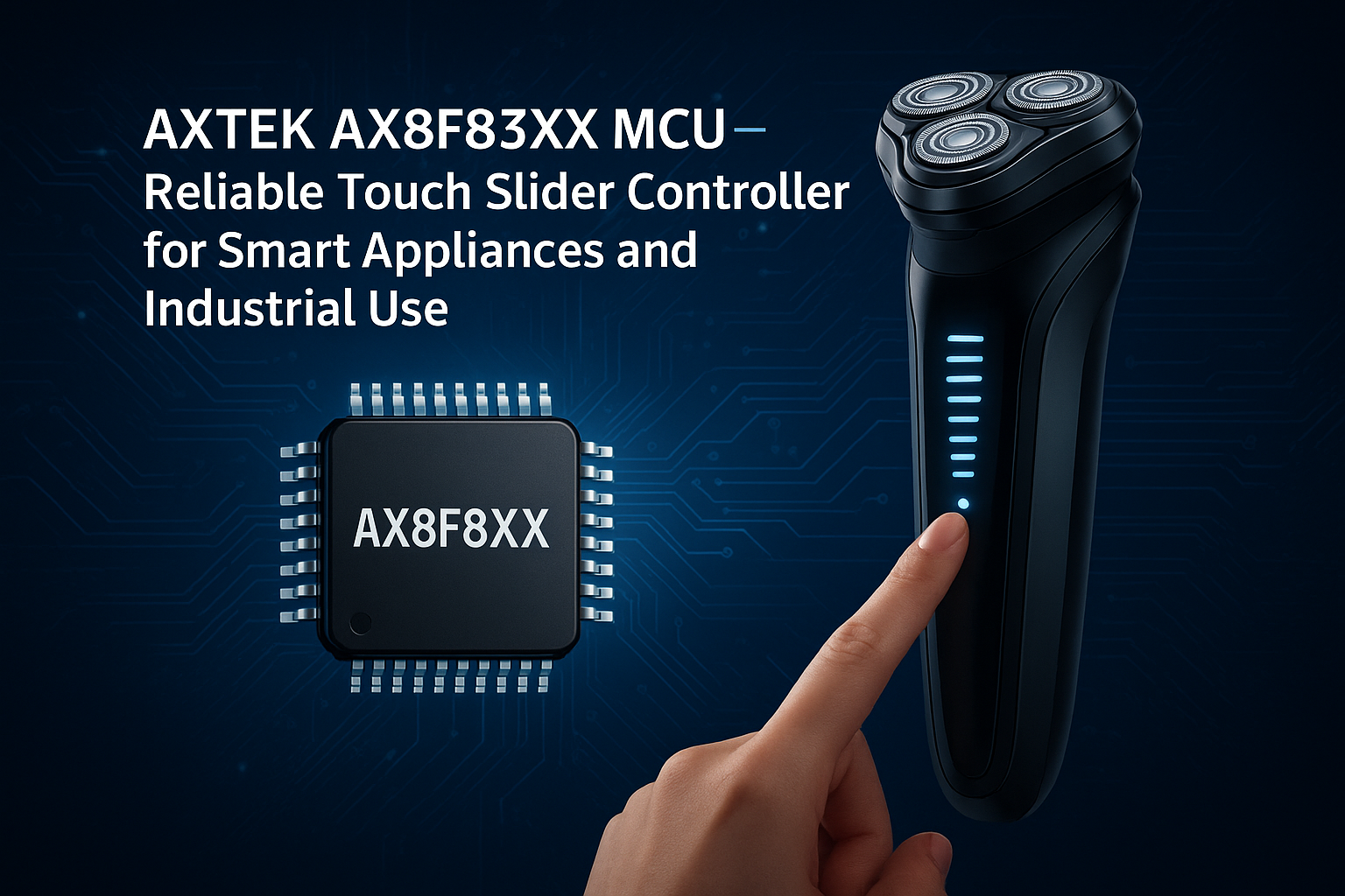
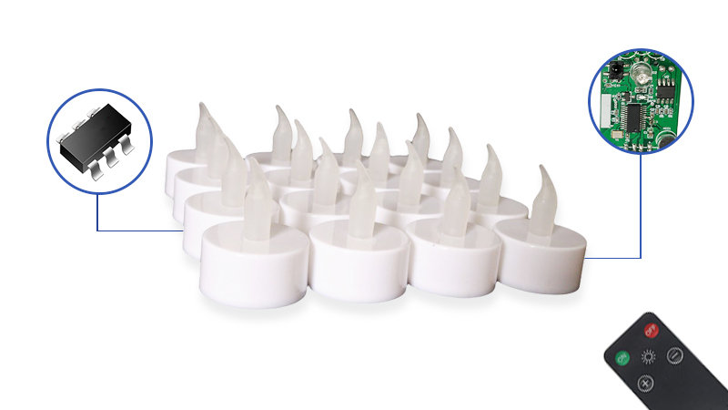
 Home Appliances
 Beauty Appliances
 Lighting
 Kid's Toys
 Security Alarm
 Health Care