Search...

General Description:
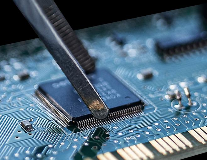
These dual N−Channel logic level enhancement mode field effecttransistors are produced using onsemi’s proprietary, high cell density,DMOS technology. This very high density process is especiallytailored to minimize on−state resistance. This device has beendesigned especially for low voltage applications as a replacement forbipolar digital transistors and small signal MOSFETs.
Features:
25 V, 0.50 A Continuous, 1.5 A Peak
RDS(ON) = 0.45 @ VGS = 4.5 V
RDS(ON) = 0.60 @ VGS = 2.7 V
Very Low Level Gate Drive Requirements Allowing DirectOperation in 3 V Circuits (VGS(th) < 1.5 V)
Gate−Source Zener for ESD Ruggedness (>6 kV Human BodyModel)
Compact Industry Standard SC70−6 Surface Mount Package These Devices are Pb−Free and are RoHS Compliant
You can get your Onsemi FDG6303N STOCK solution by flling out the form below and we will contact you immediately.
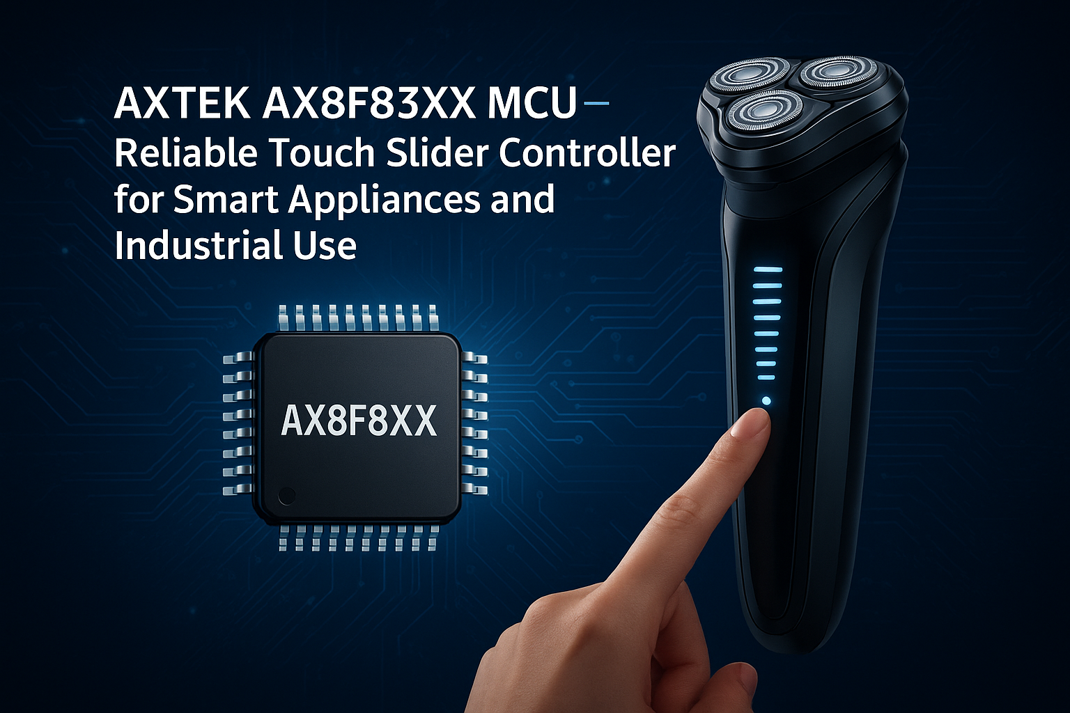
AXTEK Series NYQUEST CMSEMICON ST MICROELECTRONICS Featured Manufacturers Puya MCUs ICMAN Touch Chips ZXInfoTek Holtek MCUs MORNSUN Modules
Company Profile Certificates Terms & Conditions Privacy Statement


 MCU Solutions
 PCBA Solutions
 Bluetooth Solutions
 FAQ
FAQ Contact Us
 Company News
 Technology News
 Industry News
 PCBA News
 Company Profile
 Certificates
 Terms & Conditions
 Privacy Statement
 Home Appliances
 Beauty Appliances
 Lighting
 Kid's Toys
 Security Alarm
 Health Care