Search...



Description:
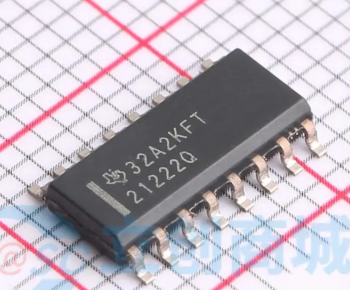
The UCC21222-Q1 device is an isolated dual-channel gate driver with programmable dead time and a wide temperature range. The device exhibits consistent performance and stability under extreme temperature conditions. It features 4-A peak source and 6-A peak sink current to drive power MOSFETs, IGBTs, and GaN transistors. The UCC21222-Q1 can be configured as two low-side drivers, two high-side drivers, or one half-bridge driver. The device's 5-ns delay matching allows two outputs to be paralleled to double drive strength under heavy-load conditions without internal shoot-through risk. The input side is isolated from the two output drivers by a 3.0-kVRMS isolation barrier, with a minimum common-mode transient immunity (CMTI) of 125 V/ns. Resistor-programmable dead time helps adjust system-limited dead time, improving efficiency and preventing output overlap. Additional protection features include: a disable function that turns off both outputs simultaneously when DIS is set high; an integrated glitch filter that rejects input transients shorter than 5 ns; and 200-ns negative voltage handling of up to –2 V on input and output pins. All supplies have UVLO protection.
Features:
Universal: dual low-side, dual high-side, or half-bridge driver
AEC-Q100 qualified with the following features:
Device temperature grade 1
Device HBM ESD classification level H2
Device CDM ESD classification level C4B
Junction temperature range: –40°C to 150°C
4-A peak source and 6-A peak sink output
Common-mode transient immunity (CMTI) greater than 125 V/ns
VDD output drive supply up to 25 V
8-V VDD UVLO
Switching parameters:
33-ns typical propagation delay
5-ns maximum pulse width distortion
10-µs maximum VDD power-up delay
UVLO protection for all supplies
Fast disable for supply sequencing
Applications:
HEV and EV battery chargers
Isolated converters in AC/DC and DC/DC power supplies
Motor drives and inverters
You can get your TI UCC21222QDRQ1 Datesheet solution by flling out the form below and we will contact you immediately.
AXTEK Series NYQUEST CMSEMICON ST MICROELECTRONICS Featured Manufacturers Puya MCUs ICMAN Touch Chips ZXInfoTek Holtek MCUs MORNSUN Modules
Company Profile Certificates Terms & Conditions Privacy Statement


 MCU Solutions
 PCBA Solutions
 Bluetooth Solutions

 FAQ
 Contact Us

 Company News
 Technology News
 Industry News
 PCBA News

 Company Profile
 Certificates
 Terms & Conditions
 Privacy Statement

 Home Appliances
 Beauty Appliances
 Lighting
 Kid's Toys
 Security Alarm
 Health Care