Search...



Description:
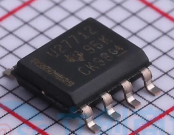
The UCC27517A-Q1 single-channel high-speed low-side gate driver device effectively drives metal-oxide-semiconductor field-effect transistor (MOSFET) and insulated-gate bipolar transistor (IGBT) switches. By virtue of an inherently designed capability to greatly reduce shoot-through current, the UCC27517A-Q1 is capable of sinking and sourcing high peak current pulses into capacitive loads, which provides rail-to-rail drive capability and extremely small propagation delay (typically 13 ns). The UCC27517A-Q1 device handles -5 V at the input. When VDD = 12 V, the UCC27517A-Q1 can provide a peak 4-A sink/source (symmetric drive) current drive capability. The UCC27517A-Q1 operates over a wide VDD range of 4.5 V to 18 V and a wide temperature range of -40°C to 140°C. The internal undervoltage lockout (UVLO) circuit on the VDD pin keeps the output low when VDD is outside the operating range. This device is capable of operating at low voltages (for example, below 5 V) and has the best-in-class switching characteristics, making it very suitable for driving newly emerging wide-bandgap power switching devices such as GaN power semiconductor devices.
Features:
Qualified for automotive applications with the following results in accordance with AEC-Q100:
125°C ambient operating temperature range
Device temperature grade 1 for automotive applications: -40°C to Grade 2
Device human body model (HBM) electrostatic discharge (ESD) classification
High-quality alternative to discrete solutions
Device charged device model (CDM) ESD classification level C6
Low-cost gate driver device provides an NPN and PNP discrete solution
4-A peak source and sink symmetric drive
Capable of handling negative voltage (-5 V) at the input
Fast propagation delay (typical 13 ns)
Fast rise and fall times (typical 9 ns and 7 ns)
4.5-V to 18-V single supply
Glitch-free pulse operation during power-up and power-down
Output held low during VDD undervoltage lockout (UVLO) (ensures
TTL- and CMOS-compatible logic thresholds (independent of supply voltage)
Hysteretic logic thresholds for high noise immunity
Dual-input design (select either an inverting (IN- pin) or non-inverting (IN+ pin) driver configuration)
An unused input pin can be used for enable or disable function
Output remains low when the input pin is floating
The maximum absolute voltage level of the input pin is not limited by the VDD pin bias supply voltage
-40°C to 140°C operating temperature range option
5-pin DBV (small outline transistor (SOT)-23) package
Applications:
Automotive
Switch-mode power supplies
DC-to-DC converters
Companion gate driver devices for digital power controllers
Solar, motor control, uninterruptible power supplies (UPS)
Gate drivers for newly emerging wide-bandgap power devices (such as GaN)
You can get your TI UCC27517AQDBVRQ1 STOCK solution by flling out the form below and we will contact you immediately.
AXTEK Series NYQUEST CMSEMICON ST MICROELECTRONICS Featured Manufacturers Puya MCUs ICMAN Touch Chips ZXInfoTek Holtek MCUs MORNSUN Modules
Company Profile Certificates Terms & Conditions Privacy Statement


 MCU Solutions
 PCBA Solutions
 Bluetooth Solutions

 FAQ
 Contact Us

 Company News
 Technology News
 Industry News
 PCBA News

 Company Profile
 Certificates
 Terms & Conditions
 Privacy Statement

 Home Appliances
 Beauty Appliances
 Lighting
 Kid's Toys
 Security Alarm
 Health Care